this post was submitted on 24 Oct 2024
93 points (100.0% liked)
Electronics
2552 readers
1 users here now
Projects, pictures, industry discussions and news about electronic engineering & component-level electronic circuits.
Rules
1: Be nice.
2: Be on-topic (eg: Electronic, not electrical).
3: No commercial stuff, buying, selling or valuations.
4: No circuit design or repair, tools or component questions.
5: No excessively promoting your own sites, social media, videos etc.
Ask questions in https://discuss.tchncs.de/c/askelectronics
founded 2 years ago
MODERATORS
you are viewing a single comment's thread
view the rest of the comments
view the rest of the comments


Is this one of those IYKYK or is there further explanation of the process involved?
Sounds amazing and fascinating but I have no idea how it's accomplished.
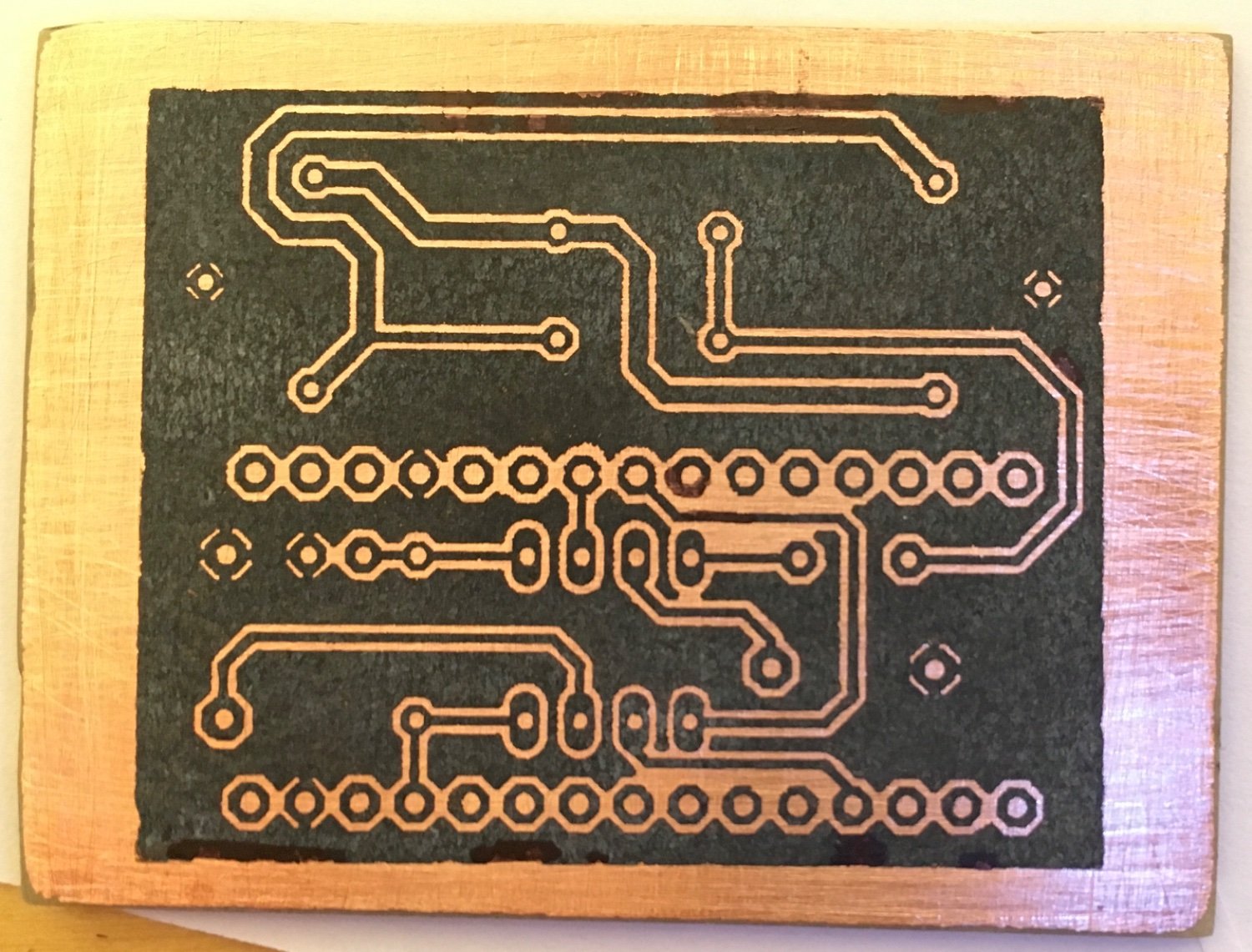
I just printed the design on a glossy paper and used an iron to transfer the toner from the paper onto the pcb (last image). The toner protects the underlying copper in the etching process, so only the free copper gets etched away. I used Na2S2O8 for etching.
I’m assuming you’re not super familiar with PCB fabrication? The toner transfer is a way to get small, repeatable, and precise definition of the component pads and traces - at home - without needing the expensive industrial machinery that fab houses have.
The toner ’print’ is a negative image, placed on a sheet of copper mounted to (usually) fiberglass. Much like masking off areas when painting, the ‘print’ protects the copper surface in select areas you want to keep safe when the whole board goes into the acid bath to dissolve the unprotected copper - leaving copper only where your ‘print’ was, and hopefully no shorts/grounds.
Definitely cool to have the ability to DIY fine pitch if you’re manually mounting SMT components or want higher board density, beats out the hand drawn permanent marker lines I’ve done in the past 😅